- HOME
- Research and Development
- R&D Organization
- Research Laboratories
- Electronic & Imaging Materials Research Laboratories
Electronic & Imaging Materials Research Laboratories
The Electronic & Imaging Materials Research Laboratories was established in 1987, and conduct the following types of research on electro-coating materials, LSI assembly materials, display materials and printing materials, and in new fields such as organic electronics, environment/energy, and medical electronics.
The Electronic & Imaging Materials Research Laboratories is a central research facility for expanding Toray's business in information and communications materials/devices, and developing materials/technology for the environment/energy and medical electronics fields. Here we create advanced materials and technologies based on our world-class technologies such as functional polymer design and synthesis, fine patterning, nano-particle dispersion, and thin-film forming.
Electro-coating
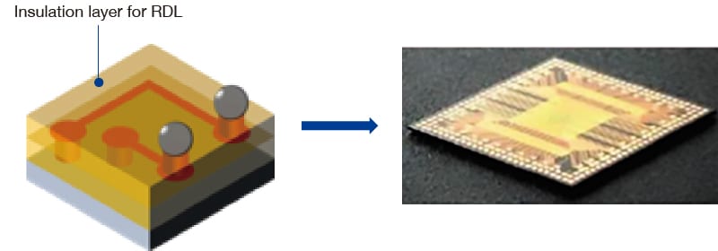
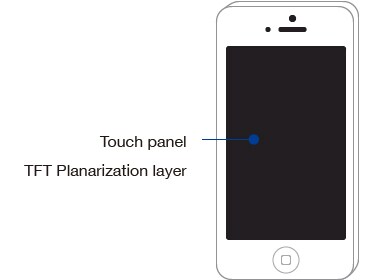
This laboratories is developing innovative materials with Toray’s unique highly heat-resistant polymers, and using these materials in protective and insulating films for semiconductors and displays, and optical transparent materials for image sensors and touch panels.
Photosensitive polyimide PHOTONEECE™
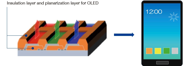
Insulation layer and planarization layer for OLED
The 2020 Commendation for Science and Technology by the Minister of Education, Culture, Sports, Science and Technology Awards for Science and Technology
LSI assembly
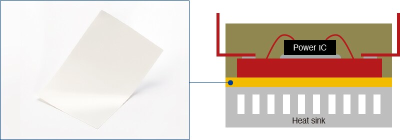
Toray is developing sheet materials with photosensitivity and high thermal conductivity, thereby helping respond to greater fineness and 3-dimensionality, and to achieve downsizing of power devices. We are also developing release layer materials for laser lift off used in micro LED manufacturing process, and photosensitive conductive materials for electrode wiring.
High thermal conductive polyimide sheet FALDA™
Displays
This laboratories has created world-class technologies ーsuch as organic light emitting display (OLED) materials and insulation materialsーfor big-screen TVs and smartphones, and is researching flexible display related materials, organic wavelength conversion materials, and other new technologies.
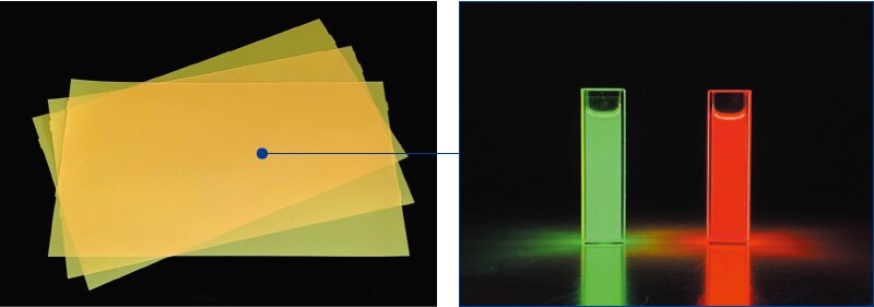
left: Backlight material
right: Spectrum conversion by organic phosphor
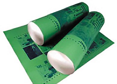
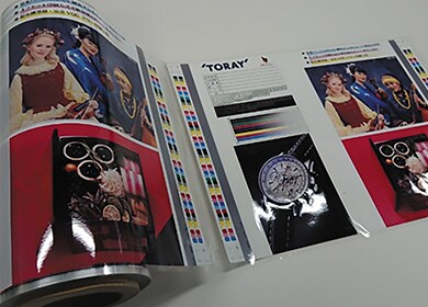
Printing
We are striving for further evolution of our unique waterless printing technology, and developing CTP (computer-to-plate) Waterless Plates for direct imaging input from computers. For film packaging, we are developing water-soluble inks, and environmentally-friendly low-CO2-emissions printing systems.
* Winner of the 2010 National Commendation for Invention Award, the Prize of the Chairman of the Japan Chamber of Commerce and Industry
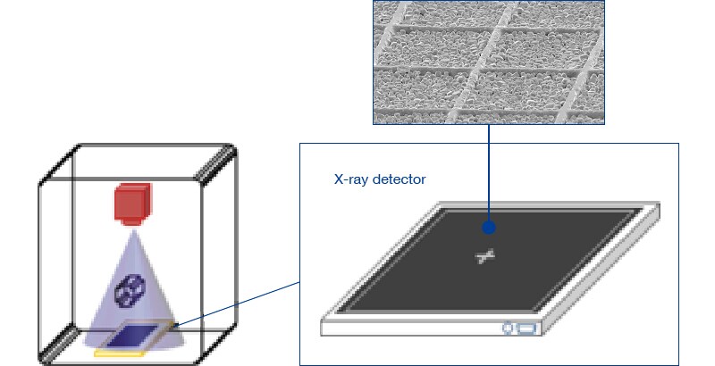
New fields
We are conducting R&D on parts for X-ray imaging equipment, next-generation communication materials, and secondary batteries, and applying these in the IoT and medical electronics fields.
Photosensitive Conductive Material
The 51st Ichimura Prize in Industry for Distinguished Achievement
Optical transparent materials
High-performance siloxane coatings PHOTOCLEAR™
The 2018 CSJ Award for Technical Development
Milestones in Toray R&D
| 1977 | Commenced production of TORELIEF™ photopolymer printing plate. |
|---|---|
| 1985 | Commenced production of polyimide coating for electronics. |
| 1987 | Established Electronic & Imaging Materials Research Laboratories. |
| 1993 | Commenced production of TOPTICAL™ color filters for liquid crystal displays. |
| 1999 | Commenced production of Toray CTP Waterless Plate. |
| 2000 | Developed PHOTONEECE™ positive photosensitive, heat-resistant, polyimide coating materials. Commenced production of PDP rear panels. |
| 2006 | Commenced production of PHOTOCLEAR™ positive photosensitive siloxane coating materials. |
| 2013 | Commenced production of photosensitive functional materials RAYBRID™ for touch panels. |
| 2017 | Developed high-performance siloxane coatings for low cure temperature. |
| 2019 | production of functional materials RAYBRID™ for vehicle navigation system. |